Okay, now we get to the bit that everyone’s been waiting for; we’re going to connect up the LEDs. Yay!
If you remember back to the original description of the board, I mentioned that there were three LEDs (next to the ESP8266 module) which, with their current-limiting resistors, were arranged in a vaguely spoked shape (and as there are only three spokes, it’s more like an old-fashioned water valve than a bicycle wheel). Unfortunately, the folks who designed the board put the LEDs on the inside of the spokes (with the resistors on the outside), which kinda’ spoils the effect …and also makes them a little more difficult to wire up, as the cathodes are all so close together. In an earlier instalment, I added a short jumper wire between GPIO5 of the ESP8266 and the cathode of the blue LED (which is the one closest to the ESP8266), simply so that I could have some indication that the module was powered on and operational. As with most quick-and-dirty hacks, it has become permanent and, despite the fact that it’s butt-ugly, I’m not planning to change it. That leaves the two others.

Going back to the photo of the wiring to switch K1, you can see the short jumper to the blue LED quite clearly. The spoke pointing directly at switch K2 is a green LED and the one pointing directly at the edge of the board is a red LED. It’s also clear from the photo that soldering wires to the cathodes of the two other LEDs would be quite challenging. Luckily, the drive for all three LEDs came from the QFP 8051 chip, so the cathodes of all three are wired to the pads where that unlucky device used to sit. Equally luckily (for my shaky-handed soldering), the pad for the blue LED is between the other two and, as the blue is already connected, it gives us a little bit of extra clearance to play with when soldering wires onto the green and red pads. The original schematic didn’t identify which LED was which, but our updated (ie:- scribbled on) version has them labelled. As you can see, the drive for the red LED is wired to pad 26 and the green to pad 28, so all we need to do is run wires from spare GPIOs on the ESP to those pads and update our test progam to use them. We’re going to use the adjacent GPIO14 and GPIO12 as our drive pins (GPIO4, on the other side of the module, is also still free, but we’re going to use that later for the connection to switch K2). For GPIO14 and GPIO12, we’ll run the wires around the rather bulky (and, for us, badly placed) smoothing cap sited between the ESP module and the edge of the board, under the DHT11 sensor and directly to the QFP pads (which are on the DHT11 side of the footprint). Again, use super-glue or tiny bits of hot-glue stick, melted with the soldering iron, to hold these (quite long) wires down to the PCB.
After completion, here’s what my board looked like.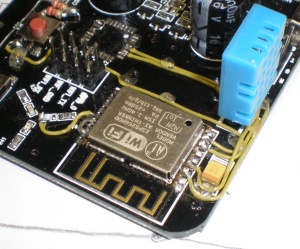 It’s starting to get a little bit crowded around that SMD capacitor, but there’s only one spare GPIO left on that side of the board anyway, so we’re not going to be adding too many more wires.
Updated code is available from the GitHub repository. The new file is named DHT11_Test_Blinken.ino and, in normal Arduino style, must be moved into a directory named DHT11_Test_Blinken to enable compilation. Note that the user_config.h file needs to be available in the same directory and that configuration changes specific to your network must be made in that file prior to compilation (ie:- your access-point SSID and password, your MQTTserver hostname and port-number, etc).
Note that if you’ve already completed the previous rework to connect switch K1 to GPIO0, you can now initiate programming mode on your T5 by turning off the power, holding down K1 and the switching the power back on again. You should be able to release K1 as soon as the board has powered up.
After programming with the “Blinken” code, the coloured LEDs will display a very brief “spinning wheel” at power-on and at all subsequent deep-sleep wake-ups.
The next instalment will cover adding K2 as a “mode control” switch, to change the function of the board at power-up time.

I love your work, I can see you have worked out quite a detailed picture of this T5 Board. I have stupid question – as I’ve started to work on the board, would you be able to give me a hint on how to connect it to TTL interface ?
I tried to connect STC_CHIP Rx and Tx but it didn’t worked out. ESP Flasher says “Note:Begin find ESP8266.” and nothing happens please help..
LikeLike
Mirek,
Yes, the RX/TX plug doesn’t seem to work at all (even for the STC chip).
There are two things you need to do to be able to access the ESP8266. The first is to enable power to it (by default it seems to be always disabled). The second is to connect directly to the RX/TX pins on the ESP8266.
– Power. You need to take the WIFI_VCC signal to ground to ensure that the
ESP8266 is powered on. If you open Part-II of the rework series
and click on the schematic, you’ll see that WIFI_VCC originates on
pin 9 of the STC chip. Jumper that to GND (pin 12 on the STC, or
any other ground point on the board) and the ESP8266 will come to life.
– RS232. The easiest way to get to RX and TX for the ESP8266 is to use the
existing jumpers on the board. Check the schematic again and then
look at your board. The RX/TX pins are routed to the four way jumper
block next to the LEDs and are clearly labelled. There’s even a nice
handy ground pin between them. PLEASE DO NOTE that these are 3v3
level TTL. You need to connect to them using a 3v3 USB adapter. A
5v USB adapter will damage the ESP8266.
Part-II and Part-III of the rework instructions give more details.
LikeLike
[…] For our next instalment, we’ll be adding long jumper wires (now that you’ve got the hang…and updating our program to implement a spinning colour wheel. Whee! Blinkenlights! […]
LikeLike
Thank you for publishing your work. The annotated schematic was quite helpful in my rebuild of this board!
Somehow AI-thinker didn’t quite acknowledge the power of the mighty ESP8266 or just wanted to push their cloud, when they designed this STC-crippled demo board. Their G6 GPRS development board has a similarly closed design.
For your information: without too much effort the mounting spot of the removed STC processor can be reused to drive all three LEDs via a WS2811 chip.
Although the SOD-8 chip is not entirely spaced the same as the STC, the original connections to the R, G and B LEDs (STC pads P2.5, P2.6 and P2.7) can be soldered to pins 1-3 of the WS2811 chip. When centering pin 2 on the middle P2.6 pad, pins 1 and 3 do cover also the adjacent pads (P2.4 and P0.0), but these are not connected, so no problem there.
Pin 4 can be soldered to the unused pads P0.1/P0.2 and can then be connected with a short wire to the GND pad on the other side. Pin 8 has no pad, but can be wired to the nearby VCC-pad.
Only pin 6 (data-in) requires a longer lead. I connected it to GPIO15 of the ESP13, (which I pulled low using a 103 SMD resistor. The original current limiting resistors on the LEDS can be removed since the WS2811 manages the LED current, but with resistors they also work. I used the Adafruit NeoPixel library, which also compiles for the ESP in the Arduino IDE.
Next to placing the WS2811 chip, I also changed the pesky red power LED. It didn’t survive removal, so I replaced it by a new led, rotated it by 135 degrees left to have it only connected on the VCC side. the GND side I connected to the ESP to function as an indicator light in addition to the R/G/B LEDs.
I preferred to stick to the original intent and also connected the buttons, the relay, the DHT and the beeper, so now my board can play the Mario theme and switch on a fan when the temperature gets too high!
I only didn’t find good use for the weird camera connector, but I still have GPIO5 available and perhaps I can combine functions of another GPIO and reuse the connector for future I2C expansions.
LikeLike
This sounds like a really interesting update Marcel. I’m sure that lots of people (including me!) will be keen to see more details. Do you have a link for schematics or pictures?
-John-
LikeLike