I before E, except after C

Working away with the hardware and software for the modified AI-Thinker T5 board, I decided that it was time to shoehorn the thing into a project case and throw it outside, to measure our night-time lows.  Following this line of thought along, I decided I’d have a go at implementing OTA (Over-The-Air) updates, as it would start to get difficult to do updates if I had to climb a ladder with a screwdriver in one hand and the laptop in the other (following the thought even further along, I realised that it was going to be pretty tough to do an OTA update on a device that sits in deep-sleep mode for 99% of the time …but we’ll cross that particular bridge if we ever get to it).  Now anyone who’s worked with any of the ESP8266 toolchains over the past year or so can probably guess what I’m going to say next.  When you change anything with the ESP, you always run into, not just another problem, but a whole extended family (including in-laws) of problems.  I haven’t found any exceptions to this rule to date and I didn’t this time, either.

I was already using v1.6.6 of the Arduino-IDE, but the ArduinoOTA program for the ESP requires v1.6.7 so, not without a little trepidation, I dutifully upgraded.  There were no massive problems.  The IDE fired up again straight away and recompiled my existing application code with n’er a murmur.  I started to get suspicious.  Where were the big red flashing warnings?  Why hadn’t my cat spontaneously combusted?  It’s too quiet!

Moving cautiously on with the plan, I opened the demo application, BasicOTA.ino, in the IDE, compiled it (successfully, again) and then, still using the USB serial adapter, squirted it to the ESP8266 on the T5.  A few seconds afterwards I saw the “Ready” message and an IP address for the board appear in the IDE serial console window.  At this point I had to heave a fairly major sigh of relief …I’d finally hit a problem …all was as it should be in the ESP world.  It was a very, very minor problem, though.  The newly minted IP address for the ESP should have shown up in the Arduino-IDE “Tools” menu as an available programmer, but it didn’t.  However, the OTA documentation warns that this might happen and suggests simply restarting the IDE, which works just fine.  After the restart, I was able to load the original DHT_Test.ino firmware to the ESP8266, hands free.  No holding down the program switch while restarting; just choose the newly available network device as the “programmer”, hit the button and away it goes.  It’s fast, too!  The OTA update only took roughly half the time of the USB method (and I’m not even counting “fiddling with switches” time).

Okay, next step.  We need (according to the documentation) to put the code for the OTA functionality into the target application itself, because the OTA code doesn’t sit in some separate, compartmentalized box somewhere in the ESP memory space, it just gets mixed right in there with everything else (so when I programmed my original DHT_Test code in that previous step as a test of the OTA functionality, it overwrote the OTA which was in memory and I lost the ability to do OTA updates again.  Duh!).

The documentation suggests that we should take the BasicOTA.ino code and just pop it into the target application, giving a fairly easy-to-follow layout, too.  So, we need to add a couple of extra includes.  Nothing too exciting there.  And then we need to add the OTA callbacks into the setup() section of the code.  This looks a bit weird to me.  I’m worried that the code in the example may have been corrupted by the markdown editor, because there are far too many square-brackets and parentheses in there.  However, the code looks the same as the BasicOTA.ino code and I know that worked, so I just quickly check with Oogleg and, having found the identical code in another tutorial, do a quick cut-and-paste.  Having dropped it into what looks approximately like the right-ish area, I save the file and, out of habit, run indent on it.  Oops! very bad move.  Indent says, “There’s far too many square-brackets and parentheses in there.  It’s given me a right headache and I’m going to puke all over your shoes.”, which it promptly did (figuratively, anyway).  After cleaning up the mess (not that difficult when you have a dog an automatic back-up file), I went back in and inserted those magic, indent incantations, /* *INDENT-OFF* */ and /* *INDENT-ON* */ above and below the weird OTA code and ran indent again, without a problem this time.

Now then, I need to put an ArduinoOTA-handle() call into the loop() section of the code.  Oh dear!  The only thing in my loop is a needlessly sarcastic comment and a call to ESP.restart(), just in case the program ever somehow, mistakenly drops through into it. Bugrit! Never mind, I’ll just try a quick compile to see whether what I already have blows anything up. Tra-la-la, IDE, reload, compile, BLAM! Futtocks! Now what?  Maybe indent was right after all!

I’m staring at a simple error message which tells me that I have an error in my lambda function (Wow! Kinky!  I don’t think I’ve ever knowingly used a lambda before) and that OTA_RECEIVE isn’t defined in this scope.  Eh?  I check that I have ArduinoOTA.h included.  I quickly check the include file itself and note that there’s an error enum define which looks okay to me.  I check the order of the includes and lose some more time re-compiling with different combinations of includes, all to no avail.  I’m just about to do what I should have done in the first place (copy the whole BasicOTA.ino file into my code and use the sections verbatim) when I got the urge to fire up “screen” and use the side-by-side mode (CTL-a followed by the pipe “|” character, if yuz didn’t already knaa) to check those small sections of code directly.  Whaddyaknow!  My cut-and-paste code, “RECEIVE”.  BasicOTA.ino, “RECIEVE”.  Bugrit!  I go back and take a closer look at the include file.  Same spelling error.  Rats!  I fire up GitHub, go to the ESP8266/Arduino/libraries/ArduinoOTA …and find that Stavros Korokithakis has already fixed it a couple of months back (thanks for that, Stavros.  The tiny ESP8266 breakout board looks great, by the way).

Onwards and upwards!  So, I fire up the library manager in my squeaky new 1.6.7 Arduino-IDE and have it update da-woyks!  I restart the IDE, fire up another compile and find that the OTA_RECEIVE error is magically gone …to be replaced by the much more verbose:-

/tmp/build319.tmp/libraries/esp-mqtt/mqtt/mqtt.c.o:(.bss.default_private_key_len+0x0): multiple definition of `default_private_key_len'
/tmp/build319.tmp/libraries/ESP8266WiFi/WiFiClientSecure.cpp.o:(.bss.default_private_key_len+0x0): first defined here
/tmp/build319.tmp/libraries/esp-mqtt/mqtt/mqtt.c.o:(.bss.default_certificate_len+0x0): multiple definition of `default_certificate_len'
/tmp/build319.tmp/libraries/ESP8266WiFi/WiFiClientSecure.cpp.o:(.bss.default_certificate_len+0x0): first defined here
collect2: error: ld returned 1 exit status

Hmmm!  I suppose that the OTA_RECEIVE was just a second cousin (think extended families).  This one is definitely a wicked uncle-Ernie, fiddling about (insert air guitar here …only old codgers need apply).

I don’t have much of a clue on where to start with this one, other than the obvious MQTT library.  Unfortunately, that particular library hasn’t been updated for a few months and definitely wasn’t changed by my library update.  I’m starting to run out of patience with the extended family though, so after some more “fiddling about” of my own, I take the path of least resistance and comment out the defines in mqtt.c.  Why that file and not the ESP8266WiFi stuff?  Well, ESP8266WiFi is core and if the lengths are defined there, they’ll get carried through to any other lib in a project which depends upon them (that might not be true in Arduino land, where you need a separate bit of hardware for networking, but I’m fairly sure I’ll be using wireless in everything I do with the ESP …and definitely if I’m using MQTT).

And finally, a clean compile.

It still doesn’t work, of course (no call to the ArduinoOTA-handle() routine), but I’ve had enough for one day and decide to end the evening on a relatively high point.


Reworking the AI-Thinker T5 – Part VII

For the last in our current series of updates, we’re going to modify the board to make switch K2 into a mode control button.  Pressing the button during power-on will initiate a simple light show (it’s going to be very simple …there are only three LEDs).

Switch K2 is the one closest to the LEDs and we’re going to wire it up to GPIO4 on the ESP module.  If you recall our previous instalment describing the rework for switch K1, you’ll remember that  we already added the 22K pull-up resistor for K2 at the same time, so this final bit of rework is simply adding one wire.Switch K2 Wiring  The photograph shows the routing for that wire, down the side of the original jumper block and then skirting K2 itself to connect to the pin on K2 which is closest to the corner of the PCB (the bare wire on the other side is the leg of the pull-up resistor).  With the previous experience of adding the LED and K1 wires, this last one should be a breeze.  The GPIO pin is on the side of the ESP module which is closest to the switch and soldering to the pins (at both the ESP and K2) is easier than trying to tack down to the QFP pads (without bridging them).  If you route the wire close to the jumper block you’ll only need a couple of right-angle turns and you’ll leave the area around the LEDs clear of any visual obstruction.  As with the previous mods, hold the wire down to the PCB with super-glue or melted hot-glue at several points along the run.

That was easy!

The updated code for the K2 “mode” switch is already available in the GitHub repository.  The code changes the power-on behaviour to add a 3-second delay (with a prompt squirted to the serial port) to allow the user to press switch K2 to go into “blinkenlights” mode.  The ESP will run a brief display on the LEDs and then automatically drop back into normal operating mode.  The other changes are:-

  • The power-on “I’m alive!” indicator has been changed to two, brief flashes of the green LED.
  • The sensor-read indicator has been changed to a single, brief flash of the red LED (Note:- the red LED may flash more than once if the ESP sees bad data coming from the DHT11 and issues a re-try).

As I mentioned at the start of this post, this will be the last of this series of updates.  We do have one free GPIO pin left and we do still have the beeper and its driver circuitry intact (a small miracle, given its history).  However, I have to admit to having no great longing to connect the two together at this moment in time.  Depending upon how the board performs over time in its primary role as a battery-operated sensor, I might decide to add the beeper functionality back in (but basically, if it continues to work without devouring too many batteries on a monthly basis, it will probably stay in-situ, as it is).

I also mentioned in a previous post that I would be using the pads freed-up by the removal of the relay and screw-down connector to add a diode (to allow the board to draw power from the 5v USB adapter), but as the batteries are holding up quite well so far (and because of the possibility of someone — me! — accidentally leaving the batteries in while the USB is connected), I’m postponing that to some, unspecified later date (a hairline this side of never), too.

Let me know how you get on with your own versions of these hardware and software mods and, if I remember, I’ll try to leave an update here every now and then to let you know how the modded T5 is holding up long term.

Update – Well, after a couple of months running this as a battery-powered sensor node I’d like to add a couple of observations.  First, the battery life isn’t great.  I’m using deep sleep of course, but I had trouble getting the wireless to reliably reconnect to the preconfigured access-point if I disabled wireless at start-up and only initialized it when I wanted to talk to the MQTT server (which would conserve more power).  Second, the DHT11 sensor is fairly crap (as many have noted before), with occasional readings being way, way off from the previous or following measurements.  I’ve recently had much better luck using a BME280 sensor unit, which also includes barometric pressure (as well as using the standard, Dallas one-wire sensors for just plain, vanilla temperature measurement).  On a slightly more positive note though, the ESP8266 sensor nodes do seem to be very reliable (given a good set of batteries) and the MQTT broadcast timestamp and generation of sensor data works very well.


Reworking the AI Thinker T5 – Part VI – Blinkenlights!

Okay, now we get to the bit that everyone’s been waiting for; we’re going to connect up the LEDs.  Yay!

If you remember back to the original description of the board, I mentioned that there were three LEDs (next to the ESP8266 module) which, with their current-limiting resistors, were arranged in a vaguely spoked shape (and as there are only three spokes, it’s more like an old-fashioned water valve than a bicycle wheel).  Unfortunately, the folks who designed the board put the LEDs on the inside of the spokes (with the resistors on the outside), which kinda’ spoils the effect …and also makes them a little more difficult to wire up, as the cathodes are all so close together.  In an earlier instalment, I added a short jumper wire between GPIO5 of the ESP8266 and the cathode of the blue LED (which is the one closest to the ESP8266), simply so that I could have some indication that the module was powered on and operational.  As with most quick-and-dirty hacks, it has become permanent and, despite the fact that it’s butt-ugly, I’m not planning to change it.  That leaves the two others.

OLYMPUS DIGITAL CAMERA
GPIO0 and GPIO2 connections

Going back to the photo of the wiring to switch K1, you can see the short jumper to the blue LED quite clearly.  The spoke pointing directly at switch K2 is a green LED and the one pointing  directly at the edge of the board is a red LED.  It’s also clear from the photo that soldering wires to the cathodes of the two other LEDs would be quite challenging.  Luckily, the drive for all three LEDs came from the QFP 8051 chip, so the cathodes of all three are wired to the pads where that unlucky device used to sit.  Equally luckily (for my shaky-handed soldering), the pad for the blue LED is between the other two and, as the blue is already connected, it gives us a little bit of extra clearance to play with when soldering wires onto the green and red pads.  The original schematic didn’t identify which LED was which, but our updated (ie:- scribbled on) version has them labelled.Annotated schematic As you can see, the drive for the red LED is wired to pad 26 and the green to pad 28, so all we need to do is run wires from spare GPIOs on the ESP to those pads and update our test progam to use them.  We’re going to use the adjacent GPIO14 and GPIO12 as our drive pins (GPIO4, on the other side of the module, is also still free, but we’re going to use that later for the connection to switch K2).  For GPIO14 and GPIO12, we’ll run the wires around the rather bulky (and, for us, badly placed) smoothing cap sited between the ESP module and the edge of the board, under the DHT11 sensor and directly to the QFP pads (which are on the DHT11 side of the footprint).  Again, use super-glue or tiny bits of hot-glue stick, melted with the soldering iron, to hold these (quite long) wires down to the PCB.

After completion, here’s what my board looked like.Red & Green LED Wiring 
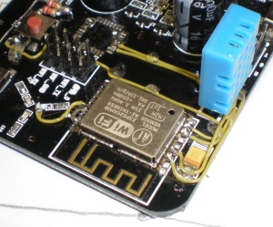
It’s starting to get a little bit crowded around that SMD capacitor, but there’s only one spare GPIO left on that side of the board anyway, so we’re not going to be adding too many more wires.

Updated code is available from the GitHub repository.  The new file is named DHT11_Test_Blinken.ino and, in normal Arduino style, must be moved into a directory named DHT11_Test_Blinken to enable compilation.  Note that the user_config.h file needs to be available in the same directory and that configuration changes specific to your network must be made in that file prior to compilation (ie:- your access-point SSID and password, your MQTTserver hostname and port-number, etc).

Note that if you’ve already completed the previous rework to connect switch K1 to GPIO0, you can now initiate programming mode on your T5 by turning off the power, holding down K1 and the switching the power back on again.  You should be able to release K1 as soon as the board has powered up.

After programming with the “Blinken” code, the coloured LEDs will display a very brief “spinning wheel” at power-on and at all subsequent deep-sleep wake-ups.

The next instalment will cover adding K2 as a “mode control” switch, to change the function of the board at power-up time.

Reworking the AI Thinker T5 – Part V

For this instalment of the rework series, we’re going to keep things simple and only do one, relatively straightforward modification.  Although there’s only one goal, it’s a relatively important one; we’re going to update one of the switches on the T5 board to provide “program” functionality for the ESP8266.  In other words, holding down the switch when you power on the board will put the module into programming mode.

The switches on the board are labelled as “K1” and “K2”.  It turns out that, after a little probing with a meter, the schematic provided for the board is incorrect, in that it shows K1 as being connected to pin-4 of the QFP chip and K2 as being connected to pin-5.  This is actually the reverse of the physical connections on the board, which actually has K1 connecting to pin-5 and K2 connecting to pin-4.   While this is immaterial in the context of this rework, it might be useful information for anyone (AI Thinker?) still trying to struggle along with the original QFP 8051 chip (I should probably add here that, despite all of my AI Thinker “bashing” in this series of posts, the vast majority of the ESP8266 modules which I own were manufactured by AI Thinker and the vast majority of them are actually great products …it’s only this one that turned out to be a stinker).

When you look at the T5 board, one of the things which is very noticeable is that there are some tiny vias and traces on the board which are signals and there are other, much larger, vias and traces which are dedicated to the power rails.  This is standard practice and it also simplifies the work of tracing signals and connections.

OLYMPUS DIGITAL CAMERA
“K1” Switch Wiring

It also gives another couple of options when trying to formulate a rework plan (how best to physically connect and route wires and place components) to give us the least amount of work for what we want to achieve.  I this particular case, a via provides a useful connection to the 3v3 supply line on the top (component) side of the board in a location which is almost ideally placed; very close to the K1 and K2 switches.  For this modification, we’re going to provide a pull-up resistor on the GPIO0 line and connect it to the K1 switch, which will become our “Program Mode” switch.  Because the via is so well placed, we’re actually going to use it to provide a second pull-up for K2 as well, but we’ll leave the actual implementation of that second switch for a later article (K2 will become the “User” switch).  So the first part of our rework modification is to add a couple of 22K resistors (this value isn’t critical, but 22K is a good compromise between stability and current draw) between VCC and the switches K1 and K2 (the other side already being connected to ground).  Looking at the photograph above, the ground connections are one the two pins of the switches furthest from the edge of the board (the pencil drawing to the left of the board shows these connected together in a continuous line).  The logic signal connections go to the two pins on each switch closest to the edge of the board.

Pull-ups first …grab two, 1/8 watt 22K resistors, hold them side by side and wrap a couple of turns of one lead from one resistor around the (still straight) lead of the other.  Solder the wrapped joint and trim back the bent lead to make it tidy.  Locate the VCC via on the board between switch K1 and the QFP pads (click on the photo above to see a larger version).  The via has a trace running to pin-10 of the QFP, so it’s easily identified.  Scrape the via clean (if needed), so that the copper is visible (a small, cross-point “plus” driver will work for this).  Bend the soldered leg of the resistor pair to a 90-degree angle, push it through the via and solder in place.  On the resistor which is closest to switch K1, cut the lead short (about 4mm), bend it into a “U” and solder it to the adjacent pin on K1 (again, see photo for details).  The long lead on the remaining resistor should be neatly bent clear of the metal casing of K1, parallel with the edge of the board and soldered to the same pin on switch K2.  You now have pull-ups on both switches.

That was the easy part.  The next bit is a little fiddly (which is why we’re only doing one).  Take some thin, single strand wire (insulated wire-wrap wire is a good choice, you might want to try varnished bell/coil wire if you’re confident that you can get the varnish coating off to tin the end reliably).

OLYMPUS DIGITAL CAMERA
“K1” Switch Wiring

We’re going to join switch K1 to GPIO0, so you need to solder one end of the wire to the second pin in on the corner of the ESP8266 next to the DHT11 sensor (I take issue with the pin numbering on these modules …if it was an IC and the antenna was the notched end, then it would be pin number 8.  If that doesn’t make any sense to you, just check the photo instead).  Note that we’ve already, in a previous posting, connected the adjacent pin, GPIO2, to the DHT11 data pin, so you  should now have two wires next to each other.  Route your new, GPIO0 wire under the DHT11, down along the side of the jumperblock and then solder it to the pin on K1 which is opposite the pin where you connected the pull-up resistor earlier.  Tack your wiring down with a couple of small drops of “Super-Glue” (if they sell it where you live …in my country of residence it’s actually an illegal substance — dunno why* — so I use toe-nail** pairings from a hot-glue gun stick, melted with the soldering iron onto the wire***).  Check your work with a meter and hopefully you’re good to go.

Why didn’t we wire up K2 as a “reset” switch?  Well, there’s already a slide switch in the supply line on the T5, so we can save switch K2 for use as a user-defined input device (yup, a “switch”).  To use your new program switch, simply turn off the power to the T5 using the slide switch; hold down switch K1 and then slide the power switch back to the “on” position.  You can let go of K1 pretty much immediately.  That’s it, you’re in program mode …you can throw away those fiddly jumpers now.

For our next instalment, we’ll be adding long jumper wires (now that you’ve got the hang of it) to connect up the green and red LEDs and updating our program to implement a spinning colour wheel.  Whee!  Blinkenlights!


  • – Perhaps the powers-that-be are scared that people will glue all of the politicians’ mouths shut.  🙂
  • Don’t use real toe-nails!
  • Don’t breathe in the fumes.  Do clean the tip of the iron ASAP.

Reworking the AI Thinker T5 – Part IV.V

The board should now be capable of running a somewhat useful program.  I’ve used the Arduino-ESP8266 core to bang this together, not because I’m an Arduino enthusiast (I’m not …I’ve never owned one, borrowed one or even stolen one), but because I found it the easiest environment to program in, given my cack-handed use of C and preference for the “vi” editor.  It just happens to handle libraries and compile code in a way which is easy to install, use and understand and it fits things into the ESP8266’s overly-complex memory footprint without requiring the user to edit SDK files.  It’s just a pity that the IDE sucks so much. 🙂

Any-hoo (see, I can speak Canadian, too!), this mini project uses the ESP8266 to interrogate the DHT11 sensor for temperature and humidity and then spits those readings out, together with a VCC voltage reading and a unique module ID, to MQTT.  After the MQTT publish is confirmed, the ESP8266 will drop into deep-sleep mode, waking itself up (assuming you remembered to connect GPIO16 to the RESET pin) after 10 minutes to start the whole process over again.

The code contains a ton of Serial.print’s, surrounded by #ifdef DEBUG #endif’s.  So as long as you have “DEBUG” defined to something in user_config.h, you’ll also see all of the data on the serial output, too.

Also in the user_config.h file are a few other settings which you must configure for your specific environment.  They include the SSID and password for your WiFi access point and static IP addresses for the ESP8266, gateway and DNS servers, as well as your MQTT server hostname, port number and topic IDs.  Everything else in that file can be tweaked too, but the items mentioned above are pretty much essential changes to get the ESP into operational mode on your specific network.

The code is available from GitHub:- PuceBaboon/ESP8266-AIT-T5

Do you need a T5 board to use this code?  Heck, no!  You can use just about any of the ESP modules out there, from the ESP-03, ESP-07, ESP-12 through to the WROOM-02.  The ESP-03 (and some of the other, older modules) may give you a bit of trouble when it comes to connecting GPIO16 to RESET, but it is doable.  The original ESP-01 is just about the only module I can’t recommend for this project.  You’ll need a DHT11 (or DHT22) and an LED to replicate the original T5 project, but all in all it’s probably easier going with a new ESP-12 than trying to rework the actual T5 board.

Libraries – The code makes use of the Adafruit DHT library and the “esp-mqtt” library from Ingo Randolf, which is a version of TuanPM’s library modded for the Arduino-ESP environment.  You’ll need to add those to your local, Arduino “libraries” directory to be able to compile the code.

A big “Thank you!” to all of those folks above for making their work available to the ESP community.

In the next instalment, we’ll do a simple update to convert one of the switches to a “program” switch (hold it down while powering on to put the ESP into programming mode) instead of having to fiddle with that jumper every time.


Reworking the AI Thinker T5 board – Part IV

I noted last time round that I wasn’t too happy with either the relay, or the red LED on our modified board, so this time we’ll take a look at the simple butchery updates needed to eliminate those particular issues, as well as updating the the hardware and the software to do something a little more useful with the board (and noting another couple of issues which cropped up along the way).

First, it’s time to heat up the soldering iron and get out the de-soldering pump again.  That relay and the associated screw-down terminal block have got to come off (the more I look at this thing, the more the idea of someone being tempted to connect mains up to it for an IoT lightbulb gives me the screaming heebie-jeebies).  The red LED is fairly inoffensive, but seeing as it sucks battery power, it’s “off with its head!” there, too.

OLYMPUS DIGITAL CAMERA
Red LED – There it was, gone!

While the LED just needs some gentle coaxing with a hot, small-tipped iron, the relay and the screw-down block do need some serious heat to de-solder the pins, so don’t expect to do the job with a 15w Antex (nice though they are) and some pre-used solder braid.  If you have one of those neat, refillable gas irons (the ones which have a catalytic heating element and run on butane lighter fuel), this is exactly the sort of job you bought it for (but a 60w rated electric iron will work, too).  Use some flux if you have it, or a tiny bit of cored solder if you don’t, so that the joints are well “wetted” before applying the de-soldering pump.  In this case (as we’re not planning on replacing, or ever using those components), it’s also acceptable to use a flat-bladed screwdriver to apply some mechanical force to the de-soldered pins to pry them away from the side of the hole (this can break the through-plating on pin holes, so don’t ever use this technique when replacing components on multi-layer boards).  When in doubt with this particular board, brute-force and ignorance are the order of the day (just remember that incessant beeping and act accordingly).

OLYMPUS DIGITAL CAMERA
Relay/screw-down removed

The end result of these mods is some extra space on the board and a drop in current consumption, too.

Keen-eyed readers will already have noticed the ugly, short yellow wire visible top-centre in this photo.  It’s a quick link I added between GPIO5 on the ESP8266 and the blue LED on the board, just to give me some extra debugging and a visible indication that the board is powered (the code in the previous article already has a few lines in there to give this LED a very quick multiple flash when power is first applied and a single short flash when the DHT11 is accessed).  Note that in the photo above, the DHT11 is now standing up vertically on the board.  This is because the heat from the ESP8266  was adding about 3C to the DHT11 readings after a few minutes of continuous use (no wonder the batteries weren’t lasting long …we were powering a space heater!).  The second part of the fix for this issue was to add another, short jumper (not visible in the photo above) between GPIO16 and the reset pin on the ESP, to enable wake from deep-sleep.  Now we can have the ESP wake itself up, take a temperature reading, then connect via WiFi to send the data to an MQTT server before going back to sleep.  Wow, something useful!

Before getting to the software, I should mention the second issue I found with the hardware (the first was the poor positioning of the DHT11 right next to the warm ESP8266).  While I was levering junk off the board with a crowbar and blowtorch, I also did some preliminary investigations into the feasibility of using the tact switches, “K1” and “K2” as reset and program buttons for the ESP.  I was looking at whether either of them had tracks or vias which were close enough to the ESP to make wiring them up quick and simple (the quick and simple answer to that is “No”).  It turns out that the silkscreen on the board and the schematic do not match.  Switch K1 is shown on the schematic as connecting to pin-4 of the QFP chip and K2 to pin-5.  In fact (on my board, anyway), it’s the other way around; K2 connects to pin-4 and K1 connects to pin-5.  That information might be useful if you’re planning to do something with K1/K2 in the future (or if you’ve got an original board which, for some obscure reason, you haven’t butchered or stamped-into-the-ground, yet).

Here’s the link to the next (short) article in the series, with the software description.


Reworking the AI Thinker T5 – Part III

In the previous post, we did some simple, straightforward modifications to get the “Black board T5” working using the ESP8266 alone.  In this part, we’ll go over a very simple application to demonstrate that the ESP8266 is alive and kicking and will download a program as normal (in program mode) and will also run that program (Duh!) and communicate with the DHT11 temperature/humidity sensor.

But first, as I mentioned in Part-II, if you have (as I do) a 5v-only USB to serial converter, you’ll need to add a 5v-to-3v3 voltage converter for the TX and RX pins, otherwise there’s a good possibility that the magic smoke will escape from your ESP8266 module.  I’m using the tried and tested MOSFET conversion method, which uses a single, N-Channel MOSFET (and two resistors) in each line to do the conversion.  You can buy these as 4-way converters on eBay for about $1 each, but the circuit is so simple that I tend to throw mine together on odd scraps of stripboard whenever I need one. For the T5 board, there’s some hardware already available which makes the stripboard method even easier.

As you’ll have noticed, there’s a nice, 5-pin connector off to one side of the board which was apparently intended as a camera port.  There aren’tOLYMPUS DIGITAL CAMERA

too many details available on what camera, or what the intended use actually was, but the important point (for us) is that pin-1 on the connector is GND and pin-5 is 3v3, with the three middle pins now free (as we’ve already removed the STC QFP micro to which those pins were connected).  By a happy coincidence, we need just exactly that number of pins to attach our 5v-to-3v3 converter (TX, RX and 5v, in addition to the existing GND and 3v3).

I’m going to show you how I implemented this connection, but as always, there are several different options available to you and you should choose whichever one is the easiest or the best match to your particular circumstances.  Some of the options you might want to consider:-

  • Find a matching plug for the camera socket and use it.
  • Remove the camera socket and replace it with pins or flying leads.
  • Ignore the socket and solder flying leads directly to existing pads.
  • Butcher the socket, because we just enjoy inflicting damage on this board (insert mandatory evil chuckle here).

Of course, I chose the last option (but in the interests of completeness I should also mention that I removed the socket from the board first,

OLYMPUS DIGITAL CAMERA
Nekkid camera socket

thinking that I would replace it with straight pins, before realizing that that was extra work and not so much fun!).  I should also mention that removing the socket is quite difficult, so I wouldn’t recommend that particular option.  Note the odd silkscreen pin descriptions which were hidden under the socket.  It seems that “CG”, “CT”, “CR” and “CV” probably stand for “Camera Ground”, “Camera Transmit”, “Camera Receive” and “Camera Volts”, respectively.

Anyway,  after consuming about twenty odd cups of tea, I had a rare flash of inspiration (in addition to the ten odd flushes) and realized that  I could just snip the top and side plastic shielding away from the existing plug and solder the chunk of stripboard with the voltage converter circuit directly to the pins (you can do this without removing the socket from the board).  Then, on the reverse side of the T5 PCB, I simply jumpered the TX and RX pins for the ESP8266 to the “WIFI_TX” and “WIFI_RX” jumper pins (described in Part-II).  The advantages of this method are, further sadistic butchery of the T5, no flying leads and the converter board is always attached to the place we want it (rather than having to search through piles of junk other projects to find it each time we want to reprogram the board).

OLYMPUS DIGITAL CAMERA

OLYMPUS DIGITAL CAMERA

The circuit for the MOSFET voltage converter can easily be found on-line by doing an Oogleg search for “MOSFET voltage level converter”.  Neither the MOSFET type nor resistor values are particularly critical in this particular application.

Okay, so we now have a board which we can program, so we need to write some software to drive it.  I’m using the Arduino-ESP core, simply because I find that it works reliably at fitting programs into the limited memory of the ESP8266 without too much faffing around on my part.  I’m not an Arduino guy (don’t own any boards, or chips) and I’m definitely not keen on the Arduino IDE, but the rest of the set up just works reliably for programming ESP8266 modules.

Here’s some code which is just a tiny bit longer than the absolute minimum to get you going with your newly modified T5 board:-

/*
* $Id: DHT_Test.ino,v 1.3 2015/12/11 02:09:02 anoncvs Exp $
*
* Test program for the AI Thinker "Black board T5", after
* modification to remove the 8051-based QFP micro and wire
* the DHT11 sensor and blue LED directly to the ESP8266.
*/
#include "DHT.h" // We're using the Adafruit version.

// DHT dht;
#define LDELAY 10 * 1000 // Loop delay (10 seconds).
#define DHTPIN 2 // DHT11 sensor on GPIO2.
ADC_MODE(ADC_VCC); // Required for correct operation of 3v3 measurement.
int BLED = 5; // Our WiFi debug LED is on GPIO5.
float temperature = 0;
float humidity = 0;

DHT dht(DHTPIN, DHT11, 15);

/*
* Turn on the blue WiFi debug LED for a short
* flash. Note that on the T5 board the LED is
* driven by a low-side switch.
*/
void BFlash() {
digitalWrite(BLED, LOW);
delay(80);
digitalWrite(BLED, HIGH);
}

/*
* Try to get a valid reading from the DHT11 sensor
* (not always easy).
*/
void getSensorData() {
temperature = dht.readTemperature();
humidity = dht.readHumidity();
while ((isnan(temperature) || isnan(humidity))
|| (temperature == 0 && humidity == 0)) {
Serial.print(“!”);
delay(500);
temperature = dht.readTemperature();
humidity = dht.readHumidity();
}
Serial.println(“”);
}

void setup() {
Serial.begin(115200);
delay(500); // Pause for boot-up crap.
pinMode(BLED, OUTPUT); // Ensure our blue LED driver pin is an output.
Serial.println();
Serial.println(“Status\tHumidity (%)\tTemperature (C)”);
dht.begin();
}

void loop() {
float vdd = ESP.getVcc() / 1000.0;
delay(LDELAY);

getSensorData();
BFlash();

Serial.println();
Serial.print(“Temperature: “);
Serial.print(temperature);
Serial.print(“c – Humidity: “);
Serial.print(humidity);
Serial.print(“% – Voltage: “);
Serial.print(vdd);
Serial.println(“v “);
}

Note that this code uses the Adafruit DHT library (please send them some of your custom  — if you happen to live on a favoured continent, you can get an Adafruit ESP8266 “Huzzah” for just about the same as you’d spend on the POJ T5 board).  This simple program doesn’t use the wireless capability of the ESP8266 at all; it just sits in a loop and squirts the temperature and humidity readings from the sensor out to the serial port every ten seconds (it also displays the current 3v3 line voltage as an added extra).

Because the T5 uses the DHT11, there’s also a while() loop in the getSensorData() function which will basically discard the (fairly frequent) bad readings returned by this particular sensor.

While we’re on the subject of the DHT11, you’ll notice when you fire up your board and start using it, that the sensor starts to read high after a few minutes.  This is because of the heat generated by the ESP8266 (which the DHT11, by a poor design choice, is sitting right next to).  You can alleviate the effects somewhat by lifting the DHT11 from its flat-on-the-board position to standing vertically, instead.  It will still read a little high (because this simple program doesn’t put the ESP8266 to sleep), but it will be noticeably better than before.

Finally, again, because the ESP8266 doesn’t sleep with this simple program and because the red, power LED is always on, the batteries will last barely 24-hours if you leave your module switched on permanently.  We’ll do something about that next time.


Reworking the AI Thinker T5 board – Part II

Please see Part 1 of this series to get up to speed on what we’ve already done (perhaps that should actually be “undone”) to get to this point.

Okay, so we’ve had our fun with the craft knife, got rid of the QFP chip and disabled the pesky beeper in the process, so what are the next steps.  My goal is to get something working in the shortest number of steps possible.  What I’d like to do is to get the DHT11 sensor working with the ESP8266 as a basic functional test and go on from there to add some of the original hardware options (LEDs, switches, etc.) back in, but again, controlled directly by the ESP8266.  I’m still (as I write this) on the fence about whether to add the beeper and the relay to that list.

The beeper came very close to being (deliberately) crushed to a messy, splintering death with a pair of pliers and I’m reluctant to give it any sort of second chance.  I can see that it might possibly be useful in some situations (locator beacon or low battery emergency alert), but for now I’ve had quite enough of it.

The relay, though …I really don’t want to encourage anyone to connect mains to this board as it stands.  There’s not enough physical clearance between the low voltage and high voltage tracks on the board, no isolating slot and, in addition, there are no mounting holes of any sort on the PCB (mains voltage on a loose board rattling around all over the shop; yuk!).  Yup, you could use it for driving a low voltage pump, or something along those lines, but most of us would probably rather use a MOSFET for something like that anyway, so at the moment the relay is slated for removal (also because I want to use the pads to mount a diode for 5v input …but more on that later).

Okay, so back to the task in hand.  What do we need to do to get the DHT11 working with the ESP8266?  There are basically three things:-

  • A connection from the DHT11 data line to an ESP8266 GPIO pin.
  • 3v3 enabled to the ESP8266.
  • Access to the ESP8266 serial port to load new firmware.

As it turns out, all three are fairly easy to implement, although the first two are rather fiddly.

T5-Schematic-AnnotatedLooking at the schematic (for what it’s worth) and at the PCB itself,  we can see that GPIO2 is fairly close to the DHT11, so we only need a

Detail
Detail of DHT11 jumper

short jumper from it to pin-3 on the DHT11 (the pull-up resistor is there already).

The power for the ESP8266 goes through a P-channel MOSFET (high-side switch), which was originally driven by pin-9 of the STC QFP chip.  Because it’s a P-channel device, we know that it needs the gate to be driven low to switch on, so instead of

OLYMPUS DIGITAL CAMERA
(Click for Full-Size)

jumpering the 3v3 directly to the ESP8266, I’m going to jumper pin-9 (on the QFP pads) to pin-12, which is ground.  This will switch the MOSFET on permanently, so whenever the board is powered on, the ESP8266 will receive power.  It also allows us to easily modify the board in the future to add our own power control for the ESP (which could be something as simple and low tech as a 555 timer, or a microswitch on a door).

The last item on the list, the connections for in-circuit programming of the ESP8266, is already taken care of by the existing jumper block (visible in the photo above).  First of all, the top jumper (with a blurry “GPIO0_”, or an upside-down “CON2”) is the standard GPIO0-jumper-to-program (so throw on a jumper to program and take it off to run normally).  The next jumper down (“WIFI_T” or  “CON5”) is the TX pin, the one below that (“WIFI_G” or “CON6”) is a GND pin and the bottom one (“WIFI_R” or “CON7”) is the RX pin.  If you have USB-to-Serial converter which has 3v3 outputs, you’re all set.  Connect TX, RX and GND to the left-hand pins of the jumper block (the pins on the same side as the coloured LED “spoke”), add a jumper to the GPIO0 pins, power cycle the board and fire up esptool.

If you don’t have a 3v3 capable USB-to-Serial converter, you’ll need to do a little extra work to add a voltage converter; we’ll get to that in Part-III (along with the test program to run on your functional DHT11 sensor module).