Implementing a wireless console using JeeLabs’ esp-link

JeeLabs have a deservedly popular ESP8266 software package, esp-link which, as with all of the best ideas, is based on a relatively simple concept, a transparent, bi-directional pass-through between serial on one side and wireless on the other.  The main thrust of their development seems to be aimed towards OTA programming of Arduinos, ARMs and even ESP8266’es, but it’s just as easy to implement a “wireless console” for a remote device and, because JeeLabs have done such a good job of creating and packaging their software, you don’t even need to compile anything; just download their package, use esptool to load it to your ESP8266 and then connect to the device over the air to configure it.  Fantastic (especially for those of us who are more comfortable with hardware than mucking around with toolchains and eagle.app.v6 files)!

Note:-  If you’re going to configure your ESP8266 device as a transparent network-to-console link, you’ll need a version with enough pins.  The ESP-12 variants are good bets for this.  You can forget trying to use the ESP-01.

What started this quest was the need to update an older headless box (a mini server without a built-in frame-buffer) and the realization that I no longer had a working machine with a serial port to connect to its console.  Like everyone else in the ESP community, I’d seen JeeLabs’ project and was impressed by their detailed write-up, so it suggested itself as both a fun project and a solution to a pressing problem.

First of all, I knew that one thing that differed from the “standard” connect-to-an-Arduino scenario was that I would be dealing with RS232 voltages, not TTL, so whatever else, I was going to need a level shifter.  Time to troll through the spares box and look for anything with “Maxim” stamped on the top.  I eventually came up with a single, unused MAX232A.  This is the version which only needs 0.1u capacitors, but has a 5v TTL interface on the inner-facing side.  Never mind, I’ll just have to throw a level shifter in there between the 3v3 ESP and the Max (this, as it turned out, would be problematic).  Other than that, I had everything else immediately to hand:-  a WROOM-02 on a project board with extra space available, the D-type connector (and even a shell) and a length of ethernet cable (saved for just such jobs after the end connectors had both lost their lock-tabs).  We were good to gStripboard with ESP8266, Max232A and level-shifterso!

I already had a couple of 2N7000 MOSFETs working as level shifters on the WROOM-02 side of the board (my USB-to-serial adapter is only 5v capable) and I added another couple next to the Max232 chip.  The odd “transistor” close to the centre edge of the board is actually a DS18B20, which was already connected up to the ESP, doing duty as a battery operated remote sensor.

One of the many neat aspects of the JeeLabs package is that the serial pins used to communicate with the target can be reassigned.  This is useful if you want to use the standard port for programming and debug, but critically, it also means that you don’t have to worry about the power-up garbage, which the ESP spews out on the standard serial port, corrupting your data stream.  As mentioned earlier, you also don’t need to re-compile to make this change; you just blow the firmware files they ship with their package to your ESP and then reconfigure it from a web browser once it comes up.

Here though I hit a problem (and I need to emphasize here that it was -my- problem and nothing at all to do with the JeeLabs package).  Whatever I did, when I first plugged my newly modified hardware into the USB adapter and fired up esptool, I just couldn’t get it to program.  I went back to using the Arduino IDE and a totally different software package …just the same.  Although the serial monitor showed what appeared to be the normal power-up crap at-a-baud-rate-no-one-else-in-the-world-can-use, it just would not program, “Connect failed”.  Well, duh!

After double checking my connections and verifying the same with the meter, I went back to the “Square Doughnuts” fault-finding procedure  (U.K. techies of a certain age will probably know what I’m talking about) and asked myself “exactly what has changed?”.  Well, obviously there’s a Max sharing the bed with the ESP now, and it connects to the ESP through a couple of MOSFET level shifters and, because I don’t want the power-up crap (at-a-baud, etc), I’m connecting it to GPIOs 13 and 15.  Ding!  Ah!  Everyone knows that GPIO-15 is super special.  Thou shalt tie it to ground at switch-on, or verily there wilt be tears!  If you’re familiar with the normal MOSFET level shifter, you’ll recall thatBasic MOSFET level-shifter the gate of the MOSFET is tied to the 3v3 rail and there’s a pull-up resistor between the gate and the source, with the source being connected to the ESP pin (GPIO-15 in our case).  Oops! Another double-Duh! moment.  By habit, I normally tie-up and tie-down using moderately low value resistors.  In this case I’d thrown in a 4k7 between GPIO-15 and ground, but there was now a 12k (“R2” in the level-shifter schematic to the left) sitting between it and 3v3.  According to our mutual friend Georg Ω, that would put the voltage on GPIO-15 very marginally into the grey area between acceptable limits for logic high and low.  It shouldn’t be enough to cause a problem, but it is borderline and obviously was causing a problem in this configuration.

One option might be to add another resistor between the gate and the 3v3 railModified level-shifter circuit and decouple it with a large-ish value capacitor (and a reverse-biased diode across the new resistor for fast discharge of the cap at switch off), which ensures that the MOSFET is clamped in the off-state at switch-on and slows down the voltage rise across the (existing) voltage divider network to ensure that GPIO-15 is pulled to ground. Once C1 has charged up through R3, the level-shifter will function as it did before.  This worked fine for me, however the real answer is to not be a cheapskate and use the proper 3v3 version of the Maxim RS232 converter chip in the first place, so that you don’t need level shifters at all.  The Max3232E is a pretty good bet (and seems to be readily available), but there are now lots of other chips withCircuit for MAX3232E - Schematic capture courtesy of CadSoft EAGLE 3v3-to-5v functionality, so you  might want to do a little sleuthing (and price comparisons) before choosing.

Firmware – As mentioned previously, the esp-link package comes with pre-built binaries (in the “firmware” directory), so you don’t need to go through the whole build process yourself.  One thing you probably do want to do though, is to make a very small modification to the supplied Makefile to prevent the “make flash” command from triggering a full rebuild automatically.  To do this simply remove the “all” dependency from the “flash:” target at around line 384 in the Makefile.  Look for this block of code:-

flash: all
$(Q) $(ESPTOOL) --port $(ESPPORT) --baud $(ESPBAUD) write_flash -fs $(ET_FS) -ff $(ET_FF) \
0x00000 "$(SDK_BASE)/bin/boot_v1.5.bin" 0x01000 $(FW_BASE)/user1.bin \
$(ET_BLANK) $(SDK_BASE)/bin/blank.bin

That first line, “flash: all“, changes to just “flash:“.  This tells make to use the existing files in the firmware directory and not to try and update them by recompiling in your environment.  Note that you may have to update the path to “ESPTOOL” (at around line 64, at the top of the Makefile), so that make can find your particular installations’ esptool.py script if it happens to be in a different location from the default.  After that you’re good to go.  Connect up your ESP8266 as normal for programming and just do “make flash“.

Once programming is complete you can restart your ESP in normal (non-programming) mode and it will automatically bring up the ESP in STA+AP mode (normal client plus access point), with the access point named something like “ESP_B3769F”.  You need to connect your WiFi to that new access-point to configure your ESP.  Once connected to the access point you can point a web browser at “192.168.4.1” to access the configuration menus.  The initial screen looks like this:-

esp-link in STA+AP mode. Top page.


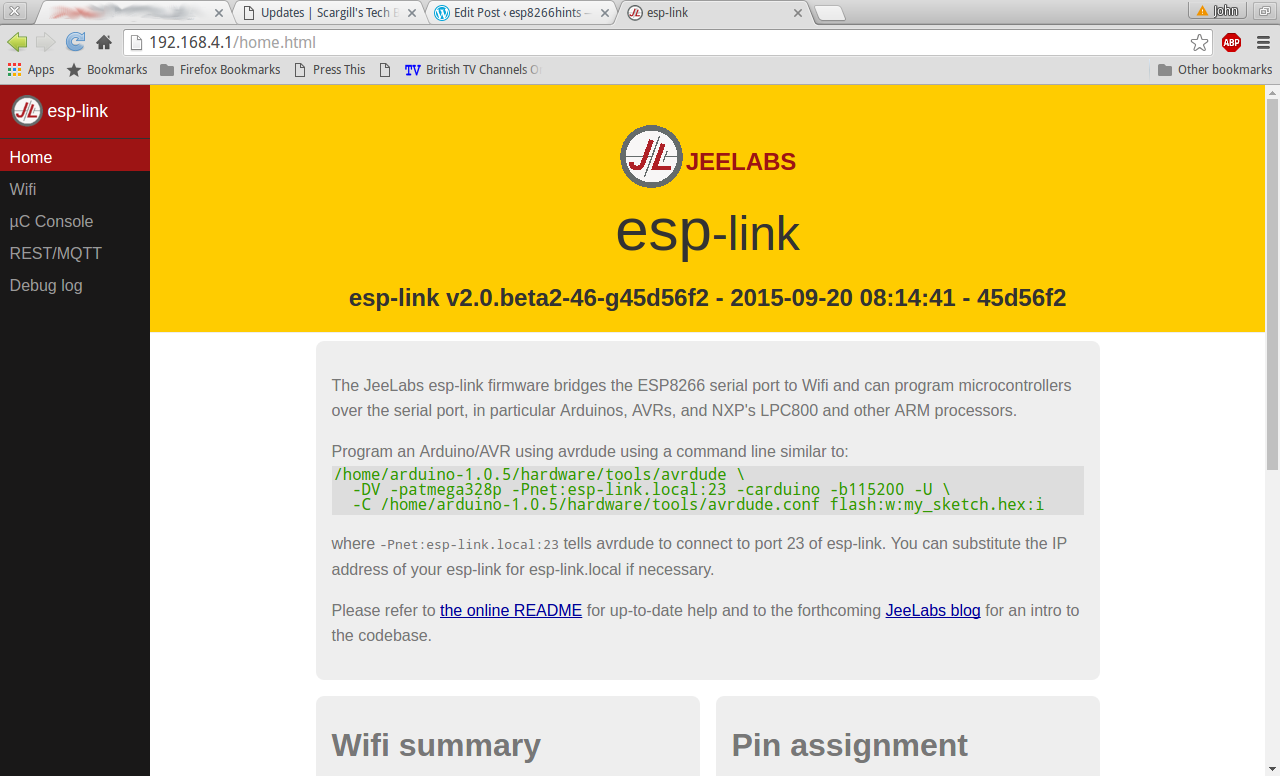
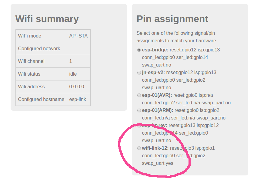
The “Pin Assignments” section on this initial page is where we’ll change the UART assignments for the console connection to our PC  (it’s important to understand that this does not change the debug output from the ESP8266, that data will still be squirted out on the normal UART-0 pins;  what it does is to redirect the “transparent” link between your network connection to the ESP and the RS232 hardware to use UART-1 on GPIO-15 and GPIO-13).  Note that there are a few different options in the pin assignment list, but only one of them (highlighted at the bottom) implements this “swap_uart” connection on alternate pins.

Option to select alternate UART pins

The other menus and set-up for configuring the device are all explained in detail in the GitHub read-me file for the project.

The baud-rate setting for your RS232 console must match the PC that you’re connecting to and that setting is at the very top of the page under the “uC Console” tab.

The “Debug log” tab shows the output from the ESP8266 console (not the RS232 device) and can be handy for initial troubleshooting.

One extra, handy function is the ability to have the ESP8266 log information to any MQTT server you have configured under the “REST/MQTT” tab.

esp-link board connected to an Alix2D3

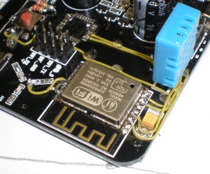
So, after all of that, does it actually work? Heck yes!  And rather well, actually.  To the left is a photo of the board connected to an Alix-2D3 (from PC-Engines) while I re-installed the software on the system (the Alix-2D3 is a headless router/gateway).   I connected the esp-link board to the console port and then, from a laptop, telnet-ed into the ESP’s address and had immediate console access (after struggling to remember the baud-rate on the Alix for a few minutes I even had console access that I could read!).  The initial installation and configuration were all done via esp-link (and it looks rather as though I’m going to have to keep this little board in my toolkit for future, headless connections).   [Aside – If you look very closely at the photograph above, you’ll notice the additional components for the programming modification around the rightmost 2N7000, next to the MAX232]

After completing the installation I went off and completely forgot about the esp-link board being still plugged in.  I came back to it 4 days later and found that the batteries were still okay and it was still quite happy to communicate via telnet, which quite surprised me (I assumed that the batteries would have been flat after a day, or maybe two at most).  Anyway, if you have a room full of servers and want a permanent console connection to each one, then you’re going to have to provide a reliable supply to the ESP board (and the ITEAD Studio PSU which I mentioned a couple of weeks back looks like a good candidate at only $2.50 a pop).

Bottom line…  A big “Thank You!” to JeeLabs for their esp-link software which helped me out in a very practical way as well as providing an entertaining and worthwhile hardware project.


Ω – “That’s Dr Ohm to thee, lad!”.

Reworking the AI-Thinker T5 – Part VII

For the last in our current series of updates, we’re going to modify the board to make switch K2 into a mode control button.  Pressing the button during power-on will initiate a simple light show (it’s going to be very simple …there are only three LEDs).

Switch K2 is the one closest to the LEDs and we’re going to wire it up to GPIO4 on the ESP module.  If you recall our previous instalment describing the rework for switch K1, you’ll remember that  we already added the 22K pull-up resistor for K2 at the same time, so this final bit of rework is simply adding one wire.Switch K2 Wiring  The photograph shows the routing for that wire, down the side of the original jumper block and then skirting K2 itself to connect to the pin on K2 which is closest to the corner of the PCB (the bare wire on the other side is the leg of the pull-up resistor).  With the previous experience of adding the LED and K1 wires, this last one should be a breeze.  The GPIO pin is on the side of the ESP module which is closest to the switch and soldering to the pins (at both the ESP and K2) is easier than trying to tack down to the QFP pads (without bridging them).  If you route the wire close to the jumper block you’ll only need a couple of right-angle turns and you’ll leave the area around the LEDs clear of any visual obstruction.  As with the previous mods, hold the wire down to the PCB with super-glue or melted hot-glue at several points along the run.

That was easy!

The updated code for the K2 “mode” switch is already available in the GitHub repository.  The code changes the power-on behaviour to add a 3-second delay (with a prompt squirted to the serial port) to allow the user to press switch K2 to go into “blinkenlights” mode.  The ESP will run a brief display on the LEDs and then automatically drop back into normal operating mode.  The other changes are:-

  • The power-on “I’m alive!” indicator has been changed to two, brief flashes of the green LED.
  • The sensor-read indicator has been changed to a single, brief flash of the red LED (Note:- the red LED may flash more than once if the ESP sees bad data coming from the DHT11 and issues a re-try).

As I mentioned at the start of this post, this will be the last of this series of updates.  We do have one free GPIO pin left and we do still have the beeper and its driver circuitry intact (a small miracle, given its history).  However, I have to admit to having no great longing to connect the two together at this moment in time.  Depending upon how the board performs over time in its primary role as a battery-operated sensor, I might decide to add the beeper functionality back in (but basically, if it continues to work without devouring too many batteries on a monthly basis, it will probably stay in-situ, as it is).

I also mentioned in a previous post that I would be using the pads freed-up by the removal of the relay and screw-down connector to add a diode (to allow the board to draw power from the 5v USB adapter), but as the batteries are holding up quite well so far (and because of the possibility of someone — me! — accidentally leaving the batteries in while the USB is connected), I’m postponing that to some, unspecified later date (a hairline this side of never), too.

Let me know how you get on with your own versions of these hardware and software mods and, if I remember, I’ll try to leave an update here every now and then to let you know how the modded T5 is holding up long term.

Update – Well, after a couple of months running this as a battery-powered sensor node I’d like to add a couple of observations.  First, the battery life isn’t great.  I’m using deep sleep of course, but I had trouble getting the wireless to reliably reconnect to the preconfigured access-point if I disabled wireless at start-up and only initialized it when I wanted to talk to the MQTT server (which would conserve more power).  Second, the DHT11 sensor is fairly crap (as many have noted before), with occasional readings being way, way off from the previous or following measurements.  I’ve recently had much better luck using a BME280 sensor unit, which also includes barometric pressure (as well as using the standard, Dallas one-wire sensors for just plain, vanilla temperature measurement).  On a slightly more positive note though, the ESP8266 sensor nodes do seem to be very reliable (given a good set of batteries) and the MQTT broadcast timestamp and generation of sensor data works very well.


Reworking the AI Thinker T5 – Part VI – Blinkenlights!

Okay, now we get to the bit that everyone’s been waiting for; we’re going to connect up the LEDs.  Yay!

If you remember back to the original description of the board, I mentioned that there were three LEDs (next to the ESP8266 module) which, with their current-limiting resistors, were arranged in a vaguely spoked shape (and as there are only three spokes, it’s more like an old-fashioned water valve than a bicycle wheel).  Unfortunately, the folks who designed the board put the LEDs on the inside of the spokes (with the resistors on the outside), which kinda’ spoils the effect …and also makes them a little more difficult to wire up, as the cathodes are all so close together.  In an earlier instalment, I added a short jumper wire between GPIO5 of the ESP8266 and the cathode of the blue LED (which is the one closest to the ESP8266), simply so that I could have some indication that the module was powered on and operational.  As with most quick-and-dirty hacks, it has become permanent and, despite the fact that it’s butt-ugly, I’m not planning to change it.  That leaves the two others.

OLYMPUS DIGITAL CAMERA
GPIO0 and GPIO2 connections

Going back to the photo of the wiring to switch K1, you can see the short jumper to the blue LED quite clearly.  The spoke pointing directly at switch K2 is a green LED and the one pointing  directly at the edge of the board is a red LED.  It’s also clear from the photo that soldering wires to the cathodes of the two other LEDs would be quite challenging.  Luckily, the drive for all three LEDs came from the QFP 8051 chip, so the cathodes of all three are wired to the pads where that unlucky device used to sit.  Equally luckily (for my shaky-handed soldering), the pad for the blue LED is between the other two and, as the blue is already connected, it gives us a little bit of extra clearance to play with when soldering wires onto the green and red pads.  The original schematic didn’t identify which LED was which, but our updated (ie:- scribbled on) version has them labelled.Annotated schematic As you can see, the drive for the red LED is wired to pad 26 and the green to pad 28, so all we need to do is run wires from spare GPIOs on the ESP to those pads and update our test progam to use them.  We’re going to use the adjacent GPIO14 and GPIO12 as our drive pins (GPIO4, on the other side of the module, is also still free, but we’re going to use that later for the connection to switch K2).  For GPIO14 and GPIO12, we’ll run the wires around the rather bulky (and, for us, badly placed) smoothing cap sited between the ESP module and the edge of the board, under the DHT11 sensor and directly to the QFP pads (which are on the DHT11 side of the footprint).  Again, use super-glue or tiny bits of hot-glue stick, melted with the soldering iron, to hold these (quite long) wires down to the PCB.

After completion, here’s what my board looked like.Red & Green LED Wiring It’s starting to get a little bit crowded around that SMD capacitor, but there’s only one spare GPIO left on that side of the board anyway, so we’re not going to be adding too many more wires.

Updated code is available from the GitHub repository.  The new file is named DHT11_Test_Blinken.ino and, in normal Arduino style, must be moved into a directory named DHT11_Test_Blinken to enable compilation.  Note that the user_config.h file needs to be available in the same directory and that configuration changes specific to your network must be made in that file prior to compilation (ie:- your access-point SSID and password, your MQTTserver hostname and port-number, etc).

Note that if you’ve already completed the previous rework to connect switch K1 to GPIO0, you can now initiate programming mode on your T5 by turning off the power, holding down K1 and the switching the power back on again.  You should be able to release K1 as soon as the board has powered up.

After programming with the “Blinken” code, the coloured LEDs will display a very brief “spinning wheel” at power-on and at all subsequent deep-sleep wake-ups.

The next instalment will cover adding K2 as a “mode control” switch, to change the function of the board at power-up time.

Reworking the AI Thinker T5 – Part V

For this instalment of the rework series, we’re going to keep things simple and only do one, relatively straightforward modification.  Although there’s only one goal, it’s a relatively important one; we’re going to update one of the switches on the T5 board to provide “program” functionality for the ESP8266.  In other words, holding down the switch when you power on the board will put the module into programming mode.

The switches on the board are labelled as “K1” and “K2”.  It turns out that, after a little probing with a meter, the schematic provided for the board is incorrect, in that it shows K1 as being connected to pin-4 of the QFP chip and K2 as being connected to pin-5.  This is actually the reverse of the physical connections on the board, which actually has K1 connecting to pin-5 and K2 connecting to pin-4.   While this is immaterial in the context of this rework, it might be useful information for anyone (AI Thinker?) still trying to struggle along with the original QFP 8051 chip (I should probably add here that, despite all of my AI Thinker “bashing” in this series of posts, the vast majority of the ESP8266 modules which I own were manufactured by AI Thinker and the vast majority of them are actually great products …it’s only this one that turned out to be a stinker).

When you look at the T5 board, one of the things which is very noticeable is that there are some tiny vias and traces on the board which are signals and there are other, much larger, vias and traces which are dedicated to the power rails.  This is standard practice and it also simplifies the work of tracing signals and connections.

OLYMPUS DIGITAL CAMERA
“K1” Switch Wiring

It also gives another couple of options when trying to formulate a rework plan (how best to physically connect and route wires and place components) to give us the least amount of work for what we want to achieve.  I this particular case, a via provides a useful connection to the 3v3 supply line on the top (component) side of the board in a location which is almost ideally placed; very close to the K1 and K2 switches.  For this modification, we’re going to provide a pull-up resistor on the GPIO0 line and connect it to the K1 switch, which will become our “Program Mode” switch.  Because the via is so well placed, we’re actually going to use it to provide a second pull-up for K2 as well, but we’ll leave the actual implementation of that second switch for a later article (K2 will become the “User” switch).  So the first part of our rework modification is to add a couple of 22K resistors (this value isn’t critical, but 22K is a good compromise between stability and current draw) between VCC and the switches K1 and K2 (the other side already being connected to ground).  Looking at the photograph above, the ground connections are one the two pins of the switches furthest from the edge of the board (the pencil drawing to the left of the board shows these connected together in a continuous line).  The logic signal connections go to the two pins on each switch closest to the edge of the board.

Pull-ups first …grab two, 1/8 watt 22K resistors, hold them side by side and wrap a couple of turns of one lead from one resistor around the (still straight) lead of the other.  Solder the wrapped joint and trim back the bent lead to make it tidy.  Locate the VCC via on the board between switch K1 and the QFP pads (click on the photo above to see a larger version).  The via has a trace running to pin-10 of the QFP, so it’s easily identified.  Scrape the via clean (if needed), so that the copper is visible (a small, cross-point “plus” driver will work for this).  Bend the soldered leg of the resistor pair to a 90-degree angle, push it through the via and solder in place.  On the resistor which is closest to switch K1, cut the lead short (about 4mm), bend it into a “U” and solder it to the adjacent pin on K1 (again, see photo for details).  The long lead on the remaining resistor should be neatly bent clear of the metal casing of K1, parallel with the edge of the board and soldered to the same pin on switch K2.  You now have pull-ups on both switches.

That was the easy part.  The next bit is a little fiddly (which is why we’re only doing one).  Take some thin, single strand wire (insulated wire-wrap wire is a good choice, you might want to try varnished bell/coil wire if you’re confident that you can get the varnish coating off to tin the end reliably).

OLYMPUS DIGITAL CAMERA
“K1” Switch Wiring

We’re going to join switch K1 to GPIO0, so you need to solder one end of the wire to the second pin in on the corner of the ESP8266 next to the DHT11 sensor (I take issue with the pin numbering on these modules …if it was an IC and the antenna was the notched end, then it would be pin number 8.  If that doesn’t make any sense to you, just check the photo instead).  Note that we’ve already, in a previous posting, connected the adjacent pin, GPIO2, to the DHT11 data pin, so you  should now have two wires next to each other.  Route your new, GPIO0 wire under the DHT11, down along the side of the jumperblock and then solder it to the pin on K1 which is opposite the pin where you connected the pull-up resistor earlier.  Tack your wiring down with a couple of small drops of “Super-Glue” (if they sell it where you live …in my country of residence it’s actually an illegal substance — dunno why* — so I use toe-nail** pairings from a hot-glue gun stick, melted with the soldering iron onto the wire***).  Check your work with a meter and hopefully you’re good to go.

Why didn’t we wire up K2 as a “reset” switch?  Well, there’s already a slide switch in the supply line on the T5, so we can save switch K2 for use as a user-defined input device (yup, a “switch”).  To use your new program switch, simply turn off the power to the T5 using the slide switch; hold down switch K1 and then slide the power switch back to the “on” position.  You can let go of K1 pretty much immediately.  That’s it, you’re in program mode …you can throw away those fiddly jumpers now.

For our next instalment, we’ll be adding long jumper wires (now that you’ve got the hang of it) to connect up the green and red LEDs and updating our program to implement a spinning colour wheel.  Whee!  Blinkenlights!


  • – Perhaps the powers-that-be are scared that people will glue all of the politicians’ mouths shut.  🙂
  • Don’t use real toe-nails!
  • Don’t breathe in the fumes.  Do clean the tip of the iron ASAP.

Reworking the AI Thinker T5 board

You’ll have seen from a previous posting that I was less than impressed with the AI Thinker’s “Black board T5”.

T5 board, minus QFP chip
Look Ma, no legs!

I was completely unable to get it to do anything other than make an extremely annoying noise and, judging from comments from others and postings to the AI Thinker (Non-)Support forum, I’m not alone.  However, I did mention at the beginning that the board looked worthwhile just for the parts alone, so having wasted enough time trying to get anywhere with the stock item I’m going to fire up the soldering iron and massacre the damn thing (insert evil chuckle here). 🙂

So, looking at the circuit diagram (which is just about the only document from AI Thinker that I can understand, crap though it is), it seems as though a good starting point to make something useful out of this would be to wire the DHT11 to one of the spare GPIO pins on the ESP8266 and turn it into a temperature and humidity monitor.  Not exactly novel, but better than letting a perfectly good WROOM-02 gather dust.  Oh, and along the way we’re going to rip that QFP micro off the board, too.  So, if anyone else wants to follow along here are the relevant steps.

Before starting, please take the batteries out, or disconnect the DC supply, if you were using one.  If you have anything  else connected up to the board (USB RS232 adapter, Van de Graaff generator, auxiliary power cord from a UFO, etc.), disconnect it now (or there will be tears!).

Break out the precision, surgical instruments.  Nah, forget the scalpel.  That chip is the thing that’s been beeping at us incessantly for the last couple of weeks.  We’re going to make it suffer (retribution is the name of the game!).  Grab yourself a box-cutter (or craft knife, or disposable hobby knife, or whatever they call them in your neck o’ the woods).  Nah, not that puny little pencil sharpener variety, get a nice sturdy 18mm (3/4″) one (we don’t want to hurt ourselves, we want to hurt that chip!).  Put the T5 down on a solid, non-scratchable surface (-don’t- use the coffee table – I have enough trouble with my own significant-other, I don’t need yours chasing me with a meat cleaver).  Take the jumpers off the pins in the middle of the board so that you have better access to the chip (and just to be clear here –and I’m talking really slowly now — the chip we’re referring to is the black square, about the size of the nail on your little finger, with 32 pretty little legs, sitting squat in the middle of the board, between the jumper block and that oh-so-annoying beeper).  Now take your craft knife and cut every single one of those 32 pretty little legs right off.  Take your time.  Enjoy yourself.  Just run the blade along the top of the legs as close to the body of the chip as you can.  Use a little downward force (you won’t need much) as you cut.  You’ll be able to feel the satisfying twang as each leg parts under the onslaught.  Fun, isn’t it!?!  Work your way round all four sides of the chip.  Take your time.  You’ll need to reposition the T5 board to get better access as you work (that beeper is being awkward again and the 1000uF cap and DHT11 are ganging up with it on the other side).  After working round all of the sides, you should be able to turn the board upside down and have the legless chip drop off.  If it doesn’t, you can pry the sides of the chip gently, just to find out where the stubborn connections are (don’t try to force the chip up, or you’ll damage pads and tracks) and then have another go on that side with the knife.  If all goes according to plan, you should end up with four neat rows of pins, but no chip (if you have a small, square hole in the middle of the board, you were using too much pressure on the box cutter — or you’re rich enough to afford a decent laser).

If the legs are all still neatly lined up (and none of them are touching their neighbours — nice, civilized little leggies), you can take a chance, pop the batteries back in (or reconnect the UFO) and switch it on.  You should be rewarded with blissful silence and a lit red LED.  If instead you are presented with magic smoke, loud Anglo-Saxon expletives and singed fingers (or interplanetary warfare), you should make an appointment with an Optician.

To finish off this instalment of chipocide you need a decent soldering iron with a clean tip (and, if you did the switch-on test in the last section, you should remove the batteries again now; mainly because the battery holder always drops off the work bench, dragging the T5 with it, at the most critical points of the rework operation).  As long as the iron is up to temperature, you should be able to “wipe” off the complete row of disconnected legs on each side.  There is at least one pad without a connection which may lift with its associated leg, but as long as you don’t leave the iron in once place for too long, all of the other pads should stay firmly in place.  Wipe the dead legs off the tip of your iron by running it over a very slightly damp rag before starting on the next row.  You can use your cleaned and tinned iron to clean up any solder bridges after you’ve taken off all of the legs (don’t use solder braid unless you’re really desperate; the heat needed to activate the braid will almost certainly lift the pads and permanently damage the board).  Once you’re happy with the cleaned-up pads, try the switch-on test again, before moving on to the next stage.

This one’s quite neat!

One of my long-standing favourite shops in Tokyo’s famous Akihabara district, Akizuki Denshi, has just started selling the WROOM-02 (that’s Espressif’s own version of the ESP-13, just in case you haven’t been paying attention) with an adapter PCB kit which brings out the pins to a breadboard-friendly connection.  It’s quite novel.

Akizuki Denshi WROOM-02 to 2.54mm DIL adapter board

The kit comes with the WROOM-02 already soldered onto the board, but the header pins (although included in the package) need to be soldered to the PCB by the purchaser.  The kit (including the WROOM-02) is priced at a very reasonable 680-Yen (that’s about $5.70) plus shipping.  Unfortunately, they don’t ship internationally.

They are also selling the bare PCB as a separate item for just 120-Yen ($1.00).

As you can see from the photo of the bare PCB, all of the pins are broken out to the adapter (including the three, separate grounds).  As far as I can tell from the photos and from the text, there are no pull-ups or pull-downs; just the pin connections and nothing else.

Bare PCB
Bare PCB

Akizuki have a long history of producing kits and PCBs for the hobby market in Japan and a look at the “kit wall” in their shop is a good, barometric indicator of what’s hot in the embedded community here (of course the challenge is actually managing to elbow your way in there to be able to see it).

‘nuther new something in town …you can safely ignore it!

AI Thinker have obviously been listening …but the question is, to whom.  They’ve just come up with something which they’re calling the “ESP8266 Black board T5” (their capitalization, not mine).  It looks really interesting at first glance.

ESP13/WROOM-02 AI Thinker board, with battery box
AI Thinker “Black board T5” development board with attached battery box

[Update:-  I ended up reworking this board to make it somewhat functional.  If you’re comfortable with a soldering iron, you might be interested in these notes]

There’s a relay and a couple of screw-down connectors at one side of the board and what’s obviously one of the older  (blue) DHT11 temperature/humidity sensors on another side, sitting next to an ESP13/WROOM-02 module.  Between the relay and the DHT11 is a barrel-connector for DC input, but the unit also comes with a 3-cell (AA size) battery box attached via short flying leads (the board itself is just a little bigger than the battery box).  There’s a beeper on the board and there are three LEDs arranged in a vaguely spoke (as in bicycle wheel) shape.  In addition, there are two mini “tact” switches, a couple of jumpers, a slide-type on/off switch and, sitting like a spider in the middle of its web, a mysterious, 32-pin, QFP package chip.  Etched along the edge of the board is “ESP822_IOT_DEMO” (sic) and also “AI-CLOUD INSIDE”.

As usual with the on-line auction site vendors, there’s b’grall useful information on any of the pages which I could find (and as the auction sites advertise it as an “ESP8266 Serial Development Board” it’s also next to impossible to find any useful information on the web, either).  Anyway, just looking at the board I thought it had to be worth the $10 asking price, just in parts alone.  With a bit of luck, the mystery chip might turn out to be an I2C expander or something equally useful.  Throwing caution to the winds (poor old Caution!), I added a single unit (Caution must have crawled back home again while I was surfing dBay) to the next order I made for other odds n’ends.

Tum-de-dum-de-do.  Wait for a couple of weeks.  Odds n’ends arrive, along with da’ board.

AI Thinker
AI Thinker “ESP8266 Black board T5”, with red LED visible just to the left of centre.

Hmmm…  Don’t recognize the number on the top of the mystery chip.  Never mind, throw in some batteries and slide the switch to “On”.  A red LED (which I hadn’t noticed in the pictures) lights up and, after a slight delay, the board starts to emit an annoying “Do something within the next few seconds, or I’ll explode” kinda’ beep.  I press one of the buttons.  It still beeps.  I press the other button.  It still beeps.  I switch it off, hold down one of the buttons and switch it back on.  It starts to beep again.  Same procedure, but other button.  Ahah!  a single beep and then blessed silence …for about a second, then it starts to beep again.  I rip the batteries out and throw the whole thing in a drawer (I was sorely tempted to throw it on the floor and stamp on it, but I thought I might damage the floor).

Back to the web (as there was b’grall documentation in the package, of course) and I resort to a Oogleg image search.  Oogleg’s image processing may be wonderful, but it seems to think that this PCB is a dead-ringer for all sorts of weird and wonderful stuff on the web that just happens to have a black PCB.  I finally find a link to AI Thinker’s forum and a thread which has some links to documents (Yay!), one of which seems to be an English PDF (double Yay!).

My yaying turns out to be a little premature.  The English documentation is limited to the schematic and it’s a fairly useless one, at that.  Many of the components evident on the board aren’t present on the schematic at all, labelling is haphazard, parts are wrongly identified (the 32-pin QFP is labelled as an STC15L2K16S on the schematic, but the part on the board is an STC15L2K32S2 [see below], the sensor is identified as a DH11, but the part on the board is definitely a DHT11) and plugs, sockets and jumper blocks are all depicted as unidentified rectangles.  One thing that does stand out immediately though, is that most of the GPIO pins on the ESP8266 are unconnected.  Uh-oh!

T5 Schematic
Original Schematic

A P-Channel MOSFET (top R/H corner of the schematic) gives another clue to what’s going on here.  The drive signal is labelled “WIFI_VCC”.  It’s a supply-side switch for the ESP8266 power.  The board is battery powered and it looks as though the ESP8266 is only powered up when a network connection is needed (and I recognized this simply because I’m doing the same thing with one of my ESP8266 projects, but using a DS3231 RTC module to drive the power switch).

So, it turns out that AI Thinker have produced a board which has a “master” microcontroller and is using the ESP8266 simply as a network interface.

Next to the on/off slide switch there’s a three-pin connector (barely visible in the photo above – it’s slightly above and to the left of the DHT11) with the silkscreen label “R-G-T”, which appears to be the serial port for the microcontroller (not for the ESP8266).  I pulled the unit out of the drawer again just long enough to connect up the pins and go through the press-beep-disconnect routine a few more times at various baud rates.  I didn’t ever get any indication of any output at all in the terminal window.  Zilch!  Nada!  Nutt’n!  At the same time I fired up a WiFi scan on one of my access points.  I could quite easily see my neighbours’ access points going up and down, but no indication at all that the ESP-13 on the board was ever powered-up.  Back in the drawer wi’thu useless burger!

I might possibly drag the thing out again and have a poke around with a multimeter, but not before I’ve de-soldered that bloody annoying beeper.

The microcontroller chip on the AI Thinker
The microcontroller chip on the AI Thinker “Black board T5”

As far as I can tell from the scant information available for this microcontroller part number available on the web, the chip is an 8051 derivative, with 32K of onboard flash memory.  I haven’t used an 8051 chip in twenty years and, although I’m sure there are some folks out there who will be positively salivating at the thought of an 8051 paired with an ESP8266, there will most certainly be many thousands more who will be scratching their heads and saying “WTF?”.  I’m not (and probably never will be) an AVR/Atmel kinda’ guy, but why AI Thinker would AI Think it a good idea to produce a board for the hobby market with such an odd-ball chip is beyond me.  If they’d dropped in an ATtiny85, a Propeller, an MPS430, a PIC18F/24F, or just about any low-end ARM chip they would have had the (ESP8266) world beating that proverbial path to their door.  As it is, they’re destined to get a big, red “FAIL” stamp splattered across their collective foreheads.  Anyway, if you’re at all interested, I finally found the data sheet for the chip on STC’s web site (no thanks to their total lack of indexing or search function and the quiet inclusion in one data-sheet — with a single processor ID as the only title —  of 18 different chips).  The highlights are, yes 8051 based, 32KB of flash, 2KB of SRAM,  29KB(Eh?!?) of EEPROM, 2 x UART, 3 x PWM, internal clock and 8-channel, 10-bit A-to-D.  If all of that lights your fire, then this is the board for you (and I’ll sell it to you …cheap!).

Hold on just a second; I need to go and add a “Double Duh!” category for this one.

Update – In an effort to introduce some semblance of balance into this post (and especially to note that I’m not, generally “anti” AI-Thinker), I’d like to point you at a couple of articles on one of their other boards, which actually is something of a bargain!  Just about the only thing it has in common with the “T5” is a long and overly complicated name, but you should definitely keep an eye open for the ESP12-based “Yellow Development Board”.  Apart from anything else, it has lots of nice flashing LEDs and you don’t need to resolder anything to get them working.

‘nuther new kid… hedzup!

Top view of the new, ESP8266-ESP13 -- Photo courtesy of AI-Thinker
Top view of the new, ESP8266-ESP13 — Photo courtesy of AI-Thinker

The WROOM v2 (aka ESP-13, aka ESP8266MOD) is becoming readily available on most auction sites, although hard details regarding memory/flash sizes are not easily found (rumours abound).

This little beastie uses yet another different form-factor and yet another different pinout.  The pitch of the castellated pins is 1.5mm, meaning it (along with its bretheren) doesn’t fit onto a normal breadboard and it won’t fit onto any pre-existing PCB designed for any of its predecessors, either (including the WROOM-01).

Currently, doing a search on eBay for “ESP8266” and sorting by lowest price, brings up the ESP-13 at the top of the list, with one vendor selling them at $2.89 (with free shipping).  That’s a pretty good deal even if the memory/flash sizes are still the same as the previous models.

Update #1 – Pins – The ESP-13/WROOM-02 modules have 18 pins available, as opposed to the 16 pins on the normal ESP-12 modules (yes, I know the ESP-12E has more).  However, two of the pins on the ESP-13/WROOM-02 are extra ground pins (duh!), so effectively it has the same number of pins as a standard ESP-12, but is more difficult to solder because of the reduced clearance between those pins.   😦

Update #2 – I noticed recently that these modules have started popping up from some of the Amazon vendors.  This seemed like good news, especially as the prices weren’t too much above the eBay/Alibaba ones.  The first vendor I tried had “In Stock” marked on the Amazon page and a very competitive price.  With the normal Amazon turn-around on shipping it seemed like a good deal, so I ordered a couple.  The order was mixed in with some other stuff and I got a normal, automated “We’ve received your order…” email immediately after submitting it.  Unfortunately, the next email, from the ESP13 vendor, said “Shipping via CHINA post”.  Duh!  If it looks too good to be true, it -is- too good to be true.

Well, the next (Amazon) vendor I tried had a web-shop with the same name, based in the country where I live and stating (on their shop page) that the WROOM-02 modules were in stock.  The price was a little higher (although not much) than the first vendor, but I thought I’d give them a try and see whether they shipped the ESP-13 or the WROOM-02.  This time I got the modules (via normal post-office delivery, not Amazon’s normal delivery service) two days later.  The modules were genuine WROOM-02’s.  Yay!  This vendor is here in Japan, so if you use amazon.co.jp I can recommend “Microtechnica” as a vendor (or you can go directly to their web shop at http://www.microtechnica-shop.jp/).  If you’re not in Japan, it’s still worth checking your local variant of the Amazon store to see whether the ESP8266 has started showing up; just try to make sure that any vendors you find have local stock and aren’t just “fronts” for someone shipping (slowly!) from China.

Update #3 – As per the previous update, I now have a couple of different versions of this module to play with.  The first thing that I  noticed is that the ESP-13 and WROOM-02 are not identical.  The WROOM-02 has a much cleaner overall finish.  In particular, the metal RF shielding is much neater, with a brushed aluminium finish, sealed corners and a neatly trimmed and soldered bottom skirt.  The ESP-13 on the other hand, has a fairly ragged RF cover, with the uneven bottom edge of the skirt getting very close to the pins in several places.  If you’re hand-soldering these modules, the WROOM-02 is much easier to deal with.  On the ESP-13 you might want to check with a multi-meter whether there are any shorts between the pins and the RF shield.

Update #4 – Continuing on with the soldering story… Hand soldering these modules (both the ESP-13 and the WROOM-02) onto strip-board using flying leads of thin wire is a pain in the proverbial.  Because there are more (side) pins than on the ESP-12 and because they’re closer together (smaller pitch), you need to use longer flying leads (the thin wires between the strip-board and the module pins) and they need to be angled more acutely (the leads to the centre pins of the module are almost straight, but as you move out towards the ends of the modules, the distance between the strip-board hole and the corresponding module pin becomes greater and greater, requiring a longer lead with a more extreme “S” bend in it).  It’s do-able, but I wouldn’t want to do very many of them.

However, help is at hand.  Eldon R. Brown, over on his blog, has come up with a very neat adapter board design which overcomes the biggest bugbear of most of the other adapters out there, namely that the resulting module+adapter is so wide as to make it impossible to connect to on a normal solderless breadboard, as it covers all of the available holes.  Eldon’s design uses surface-mount header pins to tuck the connections back in underneath the module, giving it the effective footprint of an 18-pin DIP chip.  Nice one, Eldon!

Eldon has made his adapter available as a shared project on OSH-Park, so I’ve ordered up a few (and some of the SMD header pins, too).  I’ll let you know how things turn out with them.

Update #5 – The data-sheet from Espressif for their WROOM-02 states that the external flash memory chip used on that module is 4MB (see comments, below).